[Japanese/English/Espanol]
|
[Japanese/English/Espanol]
|
|||
| Technical Comments | |||
Feed Circuits |
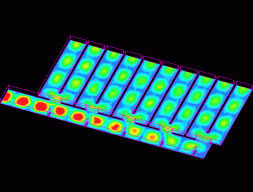
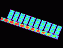
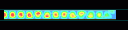
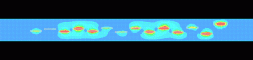
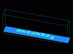
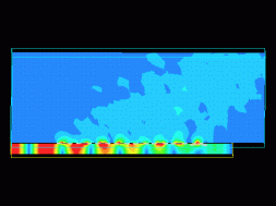
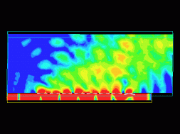
Slotted Waveguide Array |
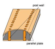
Parallel Plate Post-Wall Waveguide |
Parallel Plate
Post-Wall Waveguide
|
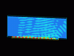
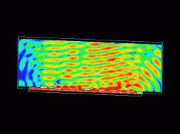
A parallel plate post-wall waveguide consists of a print circuit board (PCB) with metallized via holes, which simulate rectangular waveguide. Waveguide structures can be easily fablicated in millimeter-wave band. EM fields are concentrated in the waveguide, and do not spread like microstrip lines, which is preferable for electromagnetic compatibility (EMC). A parallel plate post-wall waveguide can reduce conductor loss by increasing the waveguide height, which is impossible using microstrip lines. A broad band post-wall waveguide to rectangular waveguide converter had been realized. For commercial use, many types of converters which connect between a post-wall waveguide and other transmission lines such as coaxial line, microstrip line and so on are required, and they are under development. A slotted parallel plate post-wall waveguide array is one of the applications of a post-wall waveguide. There are many kinds of applications such as Butler matrix, waveguide filter and other microwave circuits.
|
Microwave Circuit |
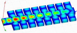
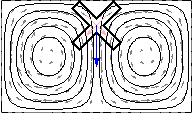
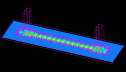
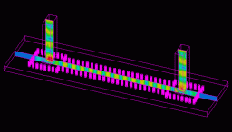
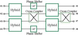
Butler Matrix
|
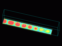
The mechanism of a Butler matrix is explained briefly using the above animation. The Butler matrix devides the input power from a port to the output ports with same amplitude but with linear phase taper. The phase taper is different for each input port. Electronic beam scanning can be realized when the Butler matrix is used as a feed circuit for antennas. The above figure shows a 4-Way Butler matrix using post-wall waveguides, whose transmission loss is much smaller than one using microstrip lines. The mechanism of a Butler matrix is understood by a discrete Fourier transform (DFT) of theDirac delta function and translation rule (F[f(t-t1)]=F[f(t)] exp(j w t1)). The Fourier transform of the Dirac delta function Dirac(t) is 1. When Dirac(t) is translated in the time domain as Dirac(t-t1), the taper in the phase is generated , and its Fourier transform becomes F[Dirac(t-t1)]=exp(j w t1) due to translation rule. Analogous to the discrete Fourier transform, let us correspond the left and right ports on the above figure to the discrete time and frequency axis, respectively. The interpretation is now clear that the output ports are the discrete Fourier transform of input ports. Butler matrix is a microwave circuit which discrete Fourier transforms analog signals. The Fast Fourier transform (FFT) algorithm is used in the Batler matrix, and it is realized by using microwave circuits such as hybrids, phase shifters and cross junctions. Systematic design procedure for the Butler matrix is well explained in the paper (T.N. Kaifas and J.N. Sahalos, "On the Design of a SIngle-Layer Wideband Butler Matrix for Switched-Beam UMTS System Applications," IEEE Antennas and Propagation Magazine, Vol.48, No.6, Dec. 2006.).
|
Comments by T. Hirano (2005.3.8)
| |
||
| Copyright(c) 2005 Ando & Hirokawa
Lab., Tokyo Institute of Technology, All Rights Reserved. |
||